Thermal Deformation Inspection Technology for Semiconductor Packages
- Mitsuhiro Ishihara
- Masatoshi Inoue
As the world's technology evolves, the precision instruments supporting that technology will also need to evolve. Today, semiconductors used in industrial products in various fields are also required to be compact, sophisticated, and highly durable in response to the trend of products becoming mobile, highly functional, and mounted on automobiles. The structure of semiconductors becomes more complex as they become more highly functional, and deformation occurs due to differences in the thermal expansion coefficients of the constituent materials, increasing the possibility of causing mechanical failure problems.
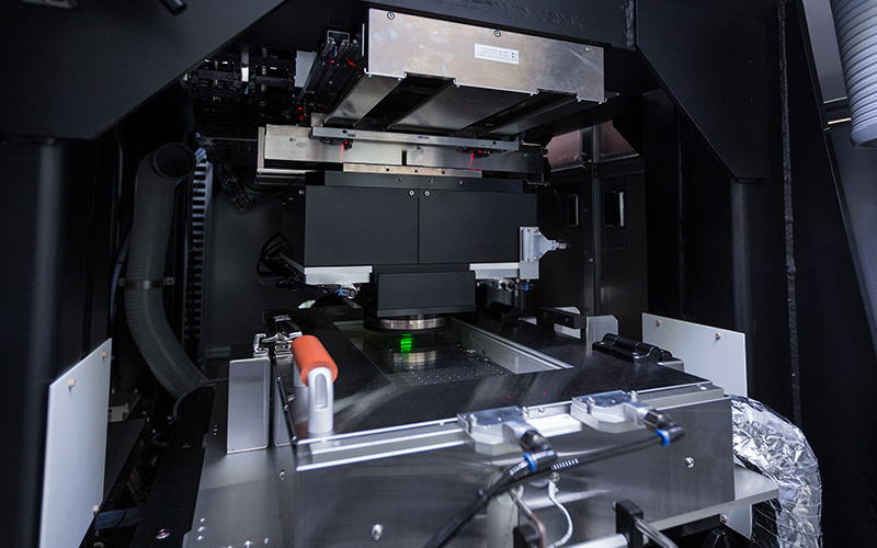
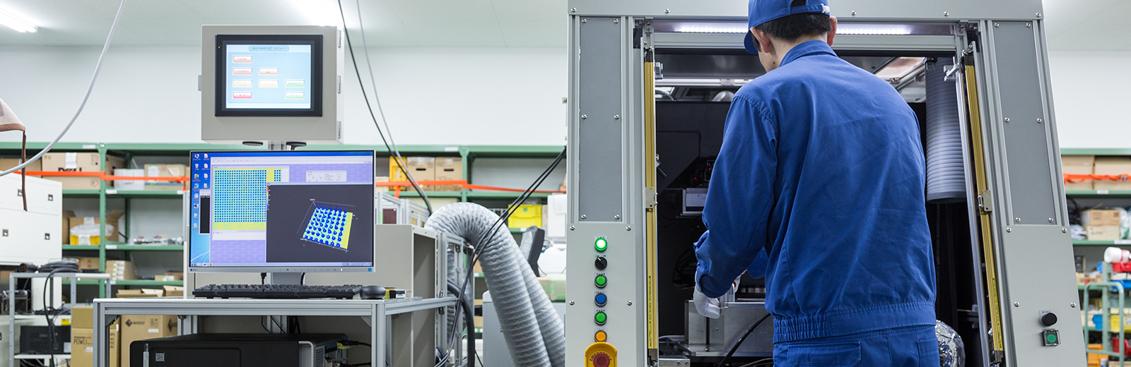
Against this background, the demand for devices that can accurately inspect and evaluate the thermal deformation characteristics of semiconductor packages is increasing year by year. TAKAOKA TOKO has developed a thermal deformation inspection device, which enables more accurate and less manpower-cost measurements, as a device for inspecting thermal deformation of semiconductor samples having a small and complex structure (hereinafter referred to as thermal deformation inspection device) by applying the technology used in the conventional in-line bump*1 height inspection device. This time, we will introduce new technologies that support the development of technology from behind.
*1) Protrusion-like microelectrodes formed on a semiconductor substrate
Technology
By using the confocal method and convection heating method, we have developed a high-precision inspection device that does not require preparation.
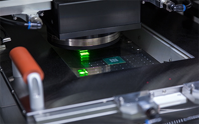
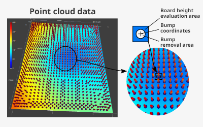
The conventional measurement method used for thermal deformation inspection device is the so-called triangulation method. Light rays are applied to the substrate surface of a semiconductor sample to be inspected, and the diffused reflected light is used for measurements. Therefore, if the diffused reflection was insufficient, measurement could not be performed successfully, and it was necessary to paint the sample manually before inspection to increase the diffused reflection. In addition, since the conventional device is based on the premise that the entire sample can be measured in a single measurement, sufficient measurement resolution cannot be ensured, and it is not possible to properly process minute parts such as bumps on the sample. Therefore, the parts must be physically removed in advance. Because of the very high manpower cost per test and the manual preparation, unintentional processing is to be performed on the substrate of even a small semiconductor sample, which can be said to have had not a minor impact on accurate measurements. The confocal method that TAKAOKA TOKO has adopted for this device is a technology cultivated in the bump height inspection device that has been developed for many years. Since this technology is originally used to measure the height and flatness of bumps, the resolution is high, and it is possible to distinguish minute parts, such as bumps, from the substrate part, to be measured, other than the bumps based on the measurement data. This eliminates the need for prior painting and removal of parts, enabling the inspection of thermal deformation of the substrate.
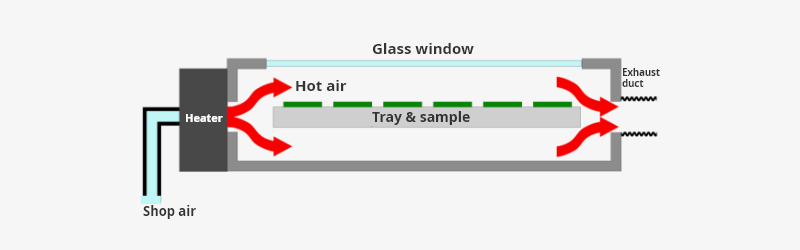
Furthermore, the heating method used to measure the thermal deformation of the sample is a convection method instead of the conventional radiation heating (heating by light) using an infrared lamp. Uniform heating of the entire sample, which has been difficult until now, has been achieved. This makes it possible to accurately inspect the deformation of semiconductor samples composed of various materials with different coefficients of thermal expansion. In addition, since semiconductor packages are heated by convection when they are mounted on motherboards, users have requested that thermal deformation inspections can be performed using the same method in order to grasp the state during mounting. This thermal deformation inspection device is also a practical one that can meet that need.
Profile
-
 Mitsuhiro IshiharaApplied Optics Inspection System Business Division
Inspection System Manufacturing Department
Director in charge Doctor of Engineering -
 Masatoshi InoueApplied Optics Inspection System Business Division
Inspection System Manufacturing Department
Development Group Chief
The confocal method cultivated in the bump height measurement technology changes the de facto standard of thermal deformation inspection.
Ishihara:The importance of thermal deformation measurement is increasing as the mobility and performance of products are rapidly progressing. As the semiconductor package itself becomes more mobile and thinner, it becomes more susceptible to deformation. In addition, as the product structure becomes more complicated due to higher performance, the difference in the expansion rate of each part also makes it easier to deform. The main cause of deformation is "heat", but as the operating speed of products increases, it becomes easier for them to generate heat. Since the adoption of more mobile and on-board system progresses, the surrounding temperature environment is also becoming more severe.
Inoue:In the field of measuring thermal deformation, a foreign-affiliated manufacturer's device was originally introduced as a de facto standard to each company. However, since the device used conventional triangulation measurement technology, it was not very user-friendly because it required preparation such as painting and removing bumps in order to measure deformation. The semiconductor sample itself is very fine and delicate. However, if it is preprocessed manually, it is difficult to obtain highly accurate data.
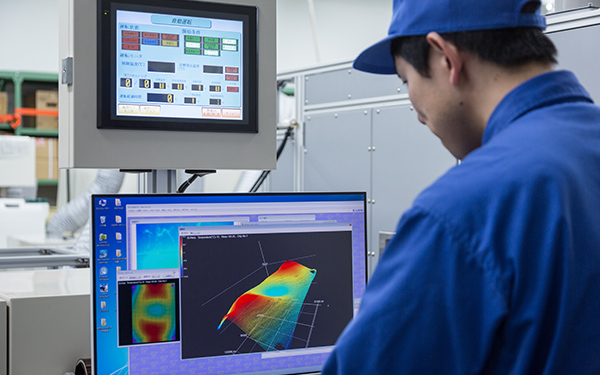
Ishihara:TAKAOKA TOKO has been working on the development of an inspection device that uses the confocal method to measure the height of the bump itself. This development was triggered by a call from a customer who used the bump height inspection device. Three-dimensional measurement technology was originally our area of expertise. Therefore, we can analyze the measured high-resolution shape point group data of the substrate surface in real time to remove unnecessary bumps for measurement on the computer. In addition, since the deformation of the substrate can be calculated digitally, manual preprocessing can be omitted, which leads to accurate measurement and reduction of manpower cost.
Inoue:The development of the first machine started in 2009. In the first place, the concept of development is different between the competitor's device and our device. Since competing products are designed as off-line analysis devices, they can be operated interactively by humans to specify the necessary parts for deformation measurement and finally obtain results. On the other hand, our device is originally based on in-line bump inspection device, so once the initial settings have been made, it is possible to measure a large number of samples fully automatically. I think that our inspection device, which can perform full automatic calculation of data including the measurement results, is very useful for customers when it is necessary to measure a large amount of sample data and derive results statistically in order to obtain highly reliable analysis results.
Continue to meet needs. That will create the future of thermal deformation inspection device.
Inoue:Another point of this thermal deformation inspection device is that it uses a convection heating method. As a result, it is now possible to uniformly heat even a sample that is a complex combination of materials with different coefficients of thermal expansion. In fact, there were also difficulties in development.
Ishihara:We already had the know-how for 3D measurement, so we knew about the measurement technology itself from the beginning of development. However, we had to start from the beginning with the heating technology. We continued trial and error while borrowing knowledge from our customers, and for the first time we adopted a radiation heating method using an infrared lamp instead of a convection method.
Inoue: From the beginning of the development, the convection method was an ideal heating method. The confocal method, a high-precision measurement method, was originally a working distance, and the distance between the measuring instrument and the object was generally short, and our measuring instruments at that time were designed taking it into account. However, when trying to heat by convection, it is necessary to put the sample inside the heating furnace, which inevitably increases the distance between the measuring instrument and the target sample.
Ishihara:We therefore gave up on using the convection method for heating at that time. However, we also received a customer's request asking us to develop a measuring device using a convection method somehow, because the convection method would be used in the manufacturing process. Through that customer, we were introduced to a manufacturer of convection heating furnaces. While borrowing the knowledge of heating, we were able to develop a measuring instrument with a long working distance and then finally complete this thermal deformation inspection device in 2016.
Inoue:Technology related to semiconductors will also continue to advance in the future. Then, the needs for inspection device will also vary. For example, there might come out demand for measurement of samples that need to be measured over a wider area with the same level of accuracy as now, and for measurement of deformation at sub-zero temperatures. We are proud that our measurement performance is at the top level in the world, but we must respond to a wide range of needs in the future.
Ishihara:The development of new measuring instruments is still progressing. As Inoue said, we want more customers to use high-performance products. To do this, it is necessary to reduce negatives in non-technical areas as much as possible. I think that the cost, the size of the device itself, and the fact that it looks cool are surely important. Of course, it is more important than anything else to improve our measurement technologies.
Latest articles
-
 interviewThe confocal surface shape measurement system for semiconductor reliabilityIt is no exaggeration to say that semiconductors are used in everything supporting our lives and industry in modern society. Examples include smartphones, home appliances, and industrial products in various fields.
 -
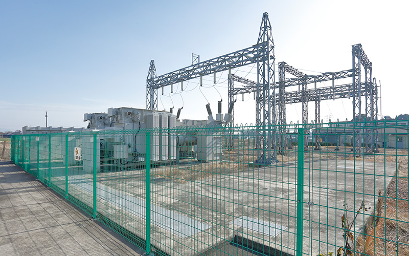 interviewImplementation of a Sensor Solution for Substation DigitalizationGlobal energy prices remain at high levels. The presumed cause is the imbalance between energy supply and demand due to recovery in economic activity from the spread of COVID-19, unseasonable weather, disasters, Russia's invasion of Ukraine, and other factors. The soaring energy prices naturally have an impact on the electricity sector, putting not only ordinary households but also electricity suppliers, or electric power companies, in a difficult situation. Power companies are being forced to cut costs to keep power prices down.
 -
 interviewDevelopment of Techniques for Solar Power Generation Prediction Using AIIn order to promote carbon neutrality, the use of renewable energy that doesn't emit CO2 is expanding.Among renewable energy resources, solar power generation is an important one which will continue to grow in popularity.
 -
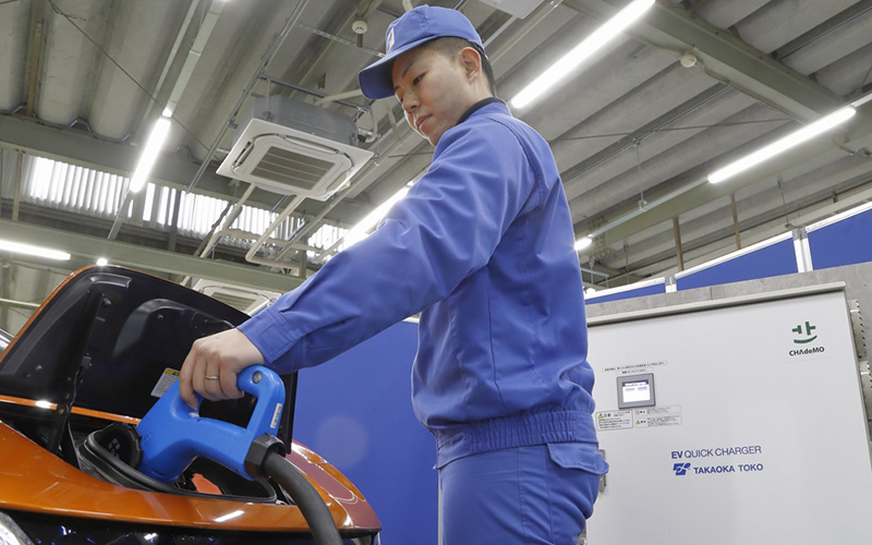 interviewDevelopment of Medium-Capacity Quick Charger for Electric VehiclesIn anticipation of expansion of EV charging infrastructure in Japan, where the EV shift is accelerating, we worked on the development of the “medium-capacity quick charger (B11)” as a charger that meets the needs for intermediate chargers between normal chargers and quick chargers. This article introduces the features of the product, ingenuity in the development process, and our future vision.