The confocal surface shape measurement system for semiconductor reliability
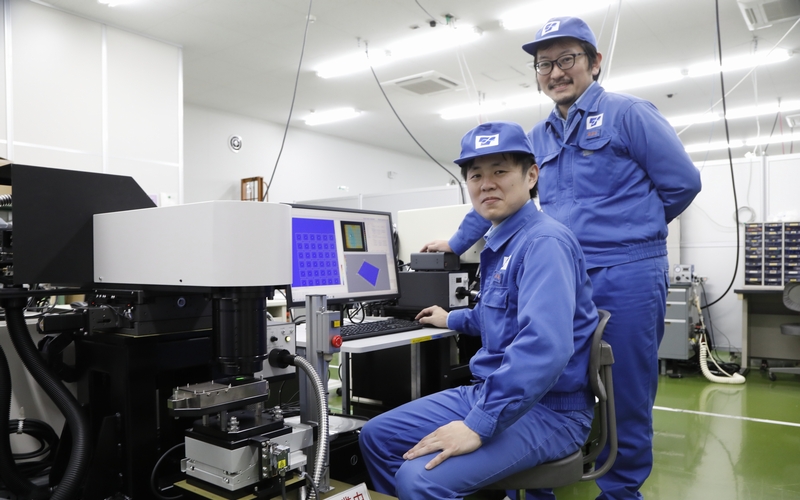
- Tatsuya Hinago
- Yuki Mizuno
It is no exaggeration to say that semiconductors are used in everything supporting our lives and industry in modern society. Examples include smartphones, home appliances, and industrial products in various fields. The Japanese government has declared that it is important to strengthen the domestic infrastructure for the development and manufacture of semiconductors in terms of economic security. Expectations are high for increased performance of and growing demand for semiconductors as exemplified by the success in attracting foreign semiconductor manufacturers and the decision by domestic semiconductor manufacturers to build their domestic plants. Semiconductor manufacturers are now required to additionally improve the reliability of semiconductors. Accordingly, the importance of inspections at the manufacturing stage will be likely to increase.
Having responded to the needs of semiconductor manufacturers for highly accurate measurement of very small objects, Takaoka Toko has offered various surface shape measurement system and inspection devices. However, management and maintenance of optical components have become more complicated as they became more diverse, making it difficult to establish a framework to achieve production volumes in response to customers' needs and to maintain the company's capability to meet the delivery time and price required by the market. Against this backdrop, we have recently developed a new surface shape measurement system that satisfies the required inspection accuracy for increasingly miniaturized semiconductors, especially for bump* height inspection, without significantly increasing the types of optical components owing to the use of existing sensors as a foundation. This article describes the features of this product, innovations in the development process, and our vision for the future.
* Protuberant electrodes formed on a semiconductor substrate package and used to achieve bonding with an IC chip.
Technology
Highly accurate surface shape measurement system newly developed while controlling the increase in optical components
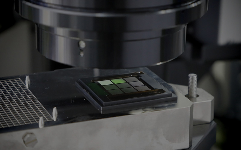
The newly developed the surface shape measurement system is installed in a bump height inspection system and is placed on the market. The bump height inspection system is used to check that the bumps on the semiconductor substrate package are correctly mounted. Improper bump mounting may adversely affect semiconductor product performance.
Takaoka Toko has developed various surface shape measurement system. However, in the manufacturing process of the surface shape measurement system, it was necessary to construct expensive jigs for each optical component (lens). The increase in the number of jigs in proportion to the types of sensor resulted in an increase in manufacturing cost and complexity of the manufacturing process.
Against this backdrop, we have developed The confocal surface shape measurement system SCS-10210R2-KN based on the existing 10000 series of the surface shape measurement system. The 10000 series accommodate different specifications by changing the combination of optical systems without increasing the number of their types. The newly developed SCS-10210R2 has a smaller measurement field of view than the SCS-10000R1 of the same series. However, it is suitable to measure fine bumps with high accuracy by increasing the numerical aperture of the objective lens and also increasing xy image resolution.
With the advancement of technology, miniaturization and densification of bumps are expected to advance more and more. To keep up with such advances, we will also aim for higher resolution in the future by adopting new cameras and for higher accuracy by enhancing software correction functions.
Profile
-
 Tatsuya HinagoApplied Optics Inspection System Business Division
Inspection System Manufacturing Department
Development Group
Manager -
 Yuki MizunoApplied Optics Inspection System Business Division
Inspection System Manufacturing Department
Development Group
Chief
The surface shape measurement system using the industry's only confocal system
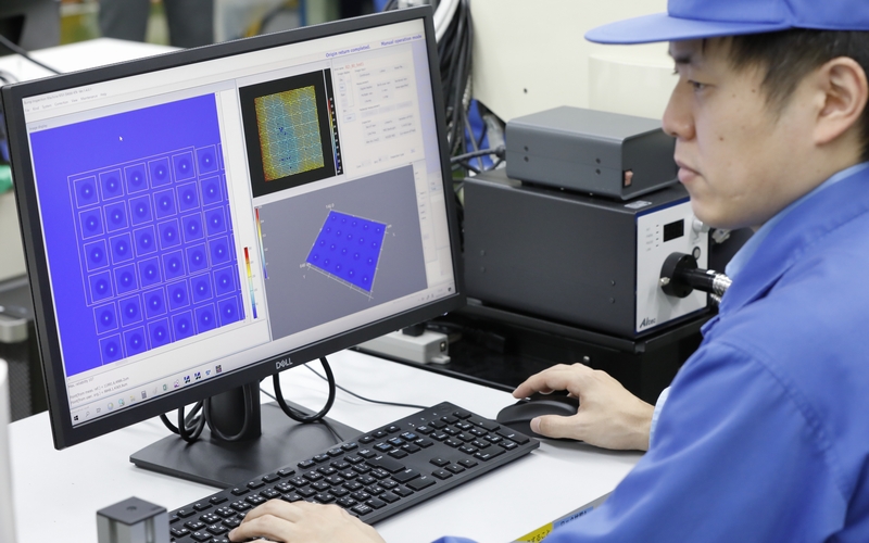
MizunoWhat we have recently developed is a sensor for inspection systems that measure the contour of objects using the confocal measurement principle. The main purpose of the equipment is to conduct visual inspections of products. One example is measurement of the height of micro-electrodes, called bumps, of semiconductor substrate packages. The substrate has rows of numerous bumps on itself. If an IC is mounted on a substrate with even a few bumps deviating in height from the designed bump height, poor contact may occur and adversely affect the performance of the semiconductor product. Inspecting substrates before IC mounting will reveal those which will cause contact failure, enabling customers to prevent yield losses through inspection.
HinagoThe substrates cost anywhere from a few thousand yen to several tens of thousands of yen each, but ICs bonded to them are more expensive, and some of them cost more than a million yen each. Once an IC is bonded, it cannot be removed, so if a contact failure occurs, the entire substrate with the IC mounted must be discarded, which results in a significant loss. If it could be determined before ICs are bonded whether the hundreds of thousands of bumps lined up on a substrate are actually aligned at the correct height of 50 or 30 micrometers, what you will need to do is simply discard the defective substrate. This is the reason why bump height inspection systems are in demand in the semiconductor market. There are bump height inspection systems from other manufacturers. Nonetheless, we are currently the only one that offers products using the confocal measurement principle. This measurement principle is one of our strengths, and the most important feature is its robustness. The measurement of very small objects is very delicate, but compared to other measurement principles, the confocal measurement principle is resistant to external noise such as vibration and enables inspection without significantly reducing speed.
MizunoThe two purposes of the current development are two: to meet the quality and speed needs in the measurement of increasingly miniaturized semiconductors and to solve the challenge that as the types of optical system increase, the number of jigs increases and their management and maintenance become more complex. Regarding the latter, using the 10000 series of existing the surface shape measurement system as a foundation, we have made it possible to support other specifications through combination modification without increasing the types of optical systems.
HinagoRegarding the former, customers are looking for faster operation in a bump height inspection system. Higher speeds are achieved by enabling the equipment to inspect a larger possible area at once. However, if you only pursue high speed, there is a trade-off that makes it impossible to measure finer details. So, faster is not necessarily better.
MizunoThe previous SCS-10000R1 had a wide 44 mm × 33 mm field of view, which was suitable for high-speed measurement of large bumps. In contrast, the new SCS-10210R2 has a field-of-view size of 15 mm × 15 mm and increased image resolution, as a sensor suitable for high-accuracy measurement of very small bumps.
HinagoWhile there are measurement sensors that have extreme advantages and disadvantages such as low accuracy but high speed and low speed but high accuracy, we are confident that the sensor we have newly developed precisely meets our customers' speed and accuracy requirements. We aim to enable as fast measurement as possible with the accuracy required by the market.
Explore future needs and provide technology and performance that satisfy customers
HinagoIt is important for us to develop, manufacture, and provide inspection equipment that meets the needs of our customers, but those needs are really difficult to identify."Are this lens, this sensor, and this accuracy really good? " "Will the customer be satisfied at this speed?” We continued to consider these issues under development. You might think that the development team is deep inside the factory, but we went to the field and had a lot of conversations with customers. Although this kind of development takes a considerable amount of time, we need to predict the current needs of next year and the year after that. That's the difficult part not only in this case but in every sensor development project. For example, we collect information and make predictions by talking to consultants and university professors, and by referring to roadmaps posted by companies at exhibitions.
MizunoThe difficult part for me in this development was bringing the lens performance to the best possible condition. The prototype lens did not achieve the same performance as the optical design simulation, and the results were not very good. Based on the verification results, the parties involved had a series of discussions about the reasons why the expected performance was not achieved and succeeded in achieving stable quality. It was truly a struggle.
HinagoWe deliver our products to customers not as discrete sensors but as packaged devices. When installed, it has been occasionally necessary to make adjustments to suit the site environment. For example, when the stage moved at high speed, the vibrations that occurred differed from what we had expected, and resonance occurred resulting in accuracy degradation. These are things that you won't know until you actually deliver the product. I think the difficulty lied in the need to speculate that far.
MizunoThese hardships and difficulties have been paid off because many customers have adopted our inspection equipment. I am certain that not only are they satisfied with the specifications, but they appreciate our responsiveness when the equipment is delivered to the site, as Hinago mentioned.
HinagoSemiconductors involve a succession of inspections. In addition to existing customers, we sometimes receive requests from new customers asking us about the feasibility of specific types of inspection. Although it is still possible to improve the accuracy of the confocal measurement principle, it may be necessary to consider methods other than the confocal measurement principle depending on customer requests.
Ensure the reliability of semiconductors to respond to the growing demand for semiconductors
MizunoWe have a senior employee who worked hard to use the confocal measurement principle and turn it into a product. It is certain that our current business is possible thanks to that person. I would also like to help my juniors like that person. In the future, I would like to be involved in development from that perspective. Regarding the future of the semiconductor industry as a whole, although demand for PCs is declining, I think demand for communication infrastructure, including smartphones, will continue to rise. In Japan, the industry and the government are working together to boost the semiconductor manufacturing capacity, so we would like to work hard as an inspection equipment manufacturer.
HinagoAs Mizuno has said, the need for semiconductors will continue to grow, and I think there is a bright future ahead where our inspection equipment will be used in more and more places. In addition to communication infrastructure, if applications that use artificial intelligence (AI) and big data, such as self-driving car technology, become commonplace in the future, semiconductors will be more widely used in the world than they are now. Specifically, semiconductor products related to autonomous driving require even greater reliability, so I think more emphasis will be placed on inspections conducted as a previous step. Accordingly, the value of our inspection equipment and the value of the company as a manufacturer should increase. Ensuring the reliability of semiconductors is the kind of work I am involved in and I am proud that the company is the place or an entity existing for that purpose. I would like to continue what I have been doing, which is development work, hoping that I will be recognized for the aforementioned kind of work, both inside and outside the company.
Latest articles
-
interviewThe confocal surface shape measurement system for semiconductor reliabilityIt is no exaggeration to say that semiconductors are used in everything supporting our lives and industry in modern society. Examples include smartphones, home appliances, and industrial products in various fields.
-
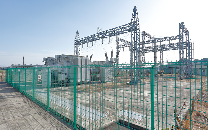 interviewImplementation of a Sensor Solution for Substation DigitalizationGlobal energy prices remain at high levels. The presumed cause is the imbalance between energy supply and demand due to recovery in economic activity from the spread of COVID-19, unseasonable weather, disasters, Russia's invasion of Ukraine, and other factors. The soaring energy prices naturally have an impact on the electricity sector, putting not only ordinary households but also electricity suppliers, or electric power companies, in a difficult situation. Power companies are being forced to cut costs to keep power prices down.
 -
 interviewDevelopment of Techniques for Solar Power Generation Prediction Using AIIn order to promote carbon neutrality, the use of renewable energy that doesn't emit CO2 is expanding.Among renewable energy resources, solar power generation is an important one which will continue to grow in popularity.
 -
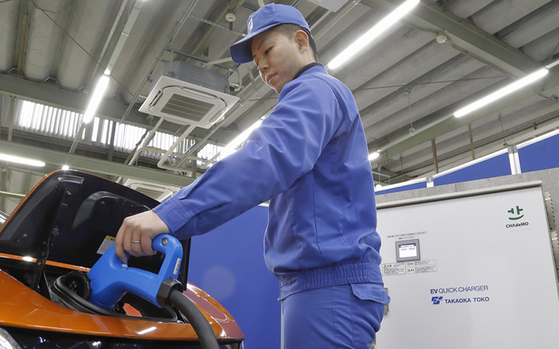 interviewDevelopment of Medium-Capacity Quick Charger for Electric VehiclesIn anticipation of expansion of EV charging infrastructure in Japan, where the EV shift is accelerating, we worked on the development of the “medium-capacity quick charger (B11)” as a charger that meets the needs for intermediate chargers between normal chargers and quick chargers. This article introduces the features of the product, ingenuity in the development process, and our future vision.