Introduction of Businesses Applied Optics Inspection System Business
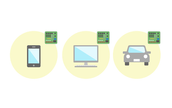
The world’s best inspection equipment uses state-of-the-art optical application technologies to support convenient products using IC packages. Our Applied Optics Inspection System Business offers inspection equipment based on unique and proprietary technologies.
The world’s best inspection equipment uses state-of-the-art optical application technologies.
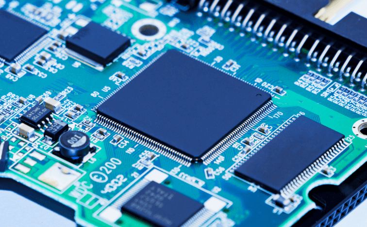
With reliable inspection technology developed from proprietary TAKAOKA TOKO technologies, our Applied Optics Inspection System Business offers inspection system can measure electrodes (bumps) instantly with a height of tends of micrometers and depth of TSVs* for use in PC CPUs and smartphones based on unique three-dimensional measurement technology that we developed. The bump inspection system can inspect more than 4,500 substrates to which thousands of bumps are mounted, respectively, every hour as the only technology in the mounting industry.
* TSV: Through Silicon Via
solution
TAKAOKA TOKO’s applied optics inspection technology
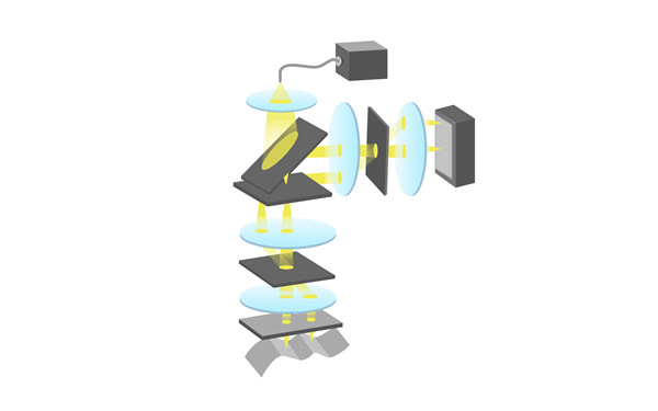
High-speed measurement cannot be expected with one-beam measurement using one pinhole. The measurement principle of TAKAOKA TOKO uses two types of multi-beam confocal optical systems (confocal method). This enables measurement with higher efficiency and reliability than conventional measurements for high-speed scanning in the light axis direction without a motion stage. At the same time, the measurement uses the light reflected from an object to measure the areas in the invisible region in the case of triangulation.
solution
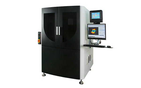
Global top manufacturer in the bump inspection field
Our system can inspect the bump height, coplanarity, and warpage of substrates, which are essential to the stable production of semiconductor product packages, to an accuracy of one micrometer at high speed and with high precision. More than 4,500 substrates to which thousands of bumps are mounted can be inspected every hour. This system made us the top global manufacturer in the field of bump height inspection.

solution
Thermal warpage inspection system
This system can measure warpage in different temperature environments at high speed and with high accuracy to verify how substrates are affected under high temperature in the substrate development processes. This system is non-destructive and no sample preparation required, which is generally needed, such as bump removal and white painting, and enables inspections with parts mounted.
solution
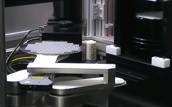
Advanced wafer micro-bump measurement technology
The 2D/3D sensor offers high accuracy and a wide field to process 2D and 3D inspections simultaneously. This technology reduces inspection time significantly, offering the best cost performance.
solution
Next-generation optics and inspection technologies
Semiconductors are increasingly required to function under wider ranges of temperature environments, such as in high-spec smartphones and automatic vehicle driving systems. With our expertise, we support future substrates for semiconductor packages.
-
 Power Equipment and System BusinessTAKAOKA TOKO realizes the building of optimum electric power plants through one-stop services that demonstrate the reliability and achievements of a company that has supported stable electric power supplies in Japan.
 -
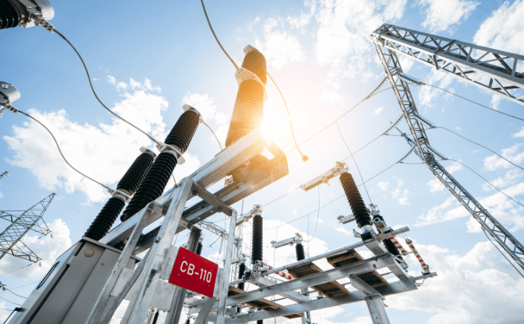
 Electric Equipment BusinessTAKAOKA TOKO supplies electric power in an optimum and efficient form, transforming high voltage to low voltage.
 -
 Measurement BusinessThrough the integration of manufacturing, logistics, and operations, the TAKAOKA TOKO Group offers next-generation electric distribution systems with its one-stop system and measurement systems.
 -
 GX Solution BusinessAs a comprehensive energy service provider, Takaoka Toko provides various solutions for facilitating the GX of the entire socioeconomic system for carbon neutrality.
 -
Applied Optics Inspection System BusinessTAKAOKA TOKO supports the manufacture of convenient products with the world’s best inspection equipment using state-of-the-art optical application technologies.