AOI (Automated Optical Inspection)Wafer Bump Inspection system WVI-S10330-RA
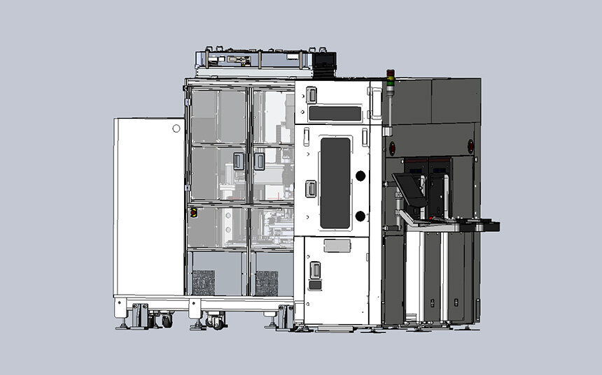
The WVI-S10330-RA is an inspection device that achieves high-speed and high-precision bump measurement of 300mm wafers utilizing the measurement technology developed through IC package substrate bump measurement.
Feature
This is an inspection device that enables high-speed and high-precision inspection of wafer bumps with a bump diameter of 12µm class.
Specifications
| Inspection item | Bump height, TTV, STV, Chip warpage, Coplanarity, Bump diameter,Bump position, Missing bump…etc. |
|---|---|
| Field of View (FOV) | About 13.0㎜×13.0㎜ |
| Inspection time | 10WPH(Depends on the conditions) |
| Z range | Max 300㎛ |
| XY Resolution | About 1.6㎛ |
| Bump diameter | Φ7.5μm~(Note 1) |
| Bump pitch | 15μm~(Note 1) |
| Accuracy in height | 3σ AVE ≦ 0.15μm *Various conditions apply |
| Dimension | (W)2,102mm×(D)2,919mm×(H)2,250mm It does not include protrusions |
Note 1 :This is target size. Pre-validation is required.
*Various conditions :TKTK standard sample (Bump diameter 20μm , Bump pitch 40μm)
Download
Download the catalog of Wafer Bump Inspection system WVI-S10330-RA.